FPGA Reaction Timer
The purpose of this project was to gain experience with a field programmable gate array (FPGA) and design of digital logic through the creation of a reaction timer. This timer must be able to wait a random length of time before measuring how long a person takes to react to an LED turning on. The purpose of this delay is to prevent someone from simply pressing a start and stop button in quick succession without ever having to truly react to an event outside of their control.
Overall Design
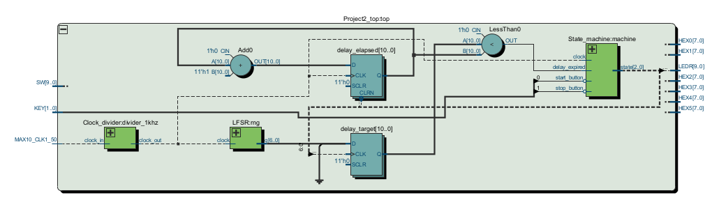
This reaction timer is built around a state machine, a pseudo-random number generator, and a counter. The random number generator is used in conjunction with a counter to create a delay of random length. At the expiration of this delay, the counter then measures the time required for the user to react and press a button. Finally, either the most recently measured reaction time or the fastest reaction time (as determined by a toggle switch) is shown on seven-segment displays.
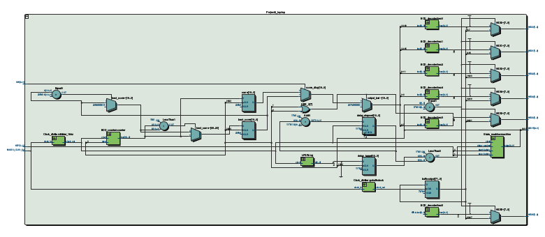
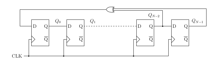
This diagram is somewhat hard to read given multiple functions all being performed in the same space. This is a simplified diagram depicting only the components used to create a random duration delay.
State Machine Design
I decided to use a zero one hot encoding of state for multiple reasons. We discussed one hot encoding in class and I liked the simplicity of logic allowing the state machine to function, but I still would have to deal with every bit being a zero when the device is initially powered on. Since I want specific actions performed when the device first powers on anyway, I decided to simply add the state where all bits are zero as one of the states.
| State[2:0] | Action |
|---|---|
| 000 | power-on |
| 001 | delay |
| 010 | count |
| 100 | result |
I also need to be able to display either the most recent reaction time or the best (shortest) reaction time, so I decided to use a Mealy type state machine. Since selection between these two output modes is done with a toggle switch, it is trivial to add a multiplexer directly using the switch input to control what value is being sent to the display drivers.
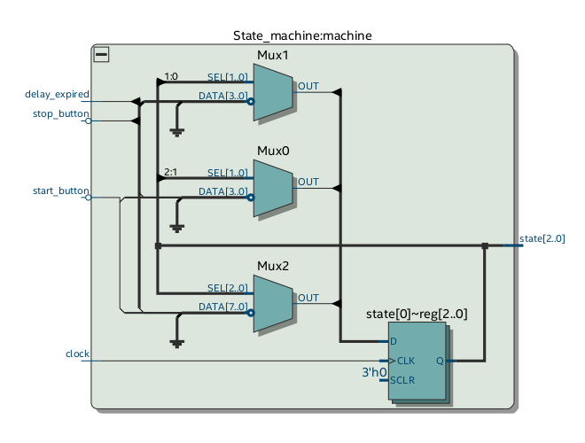
Note that both start_button and stop_button above are inverted inputs.
This is because the onboard buttons are low active.
Also note that this module does not contain the selection of which reaction time to display as the result.
Random Number Generator
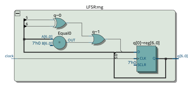
To generate pseudo-random numbers, I’m using a Fibonacci linear feedback shift register (LFSR). For this to generate pseudo-random numbers, specific numbers of bits must be used as the length of the number. For this test, I used a 7 bit LFSR.
My implementation of this shift register initally failed due to a very important misunderstanding with regards to verilog implementation in hardware.
I Iniially did not realize that inital blocks only affect simulation so my LFSR was starting with an initial condition of all zeros.
Unfortunately, this is the one stable state so it always output 0.
To fix this problem, I simply had to change the assignment of the least significant bit from d[0] = (q[N-1] ^ q[N-2]) to (q[N-1] ^ q[N-2]) || (q=={N{1'b0}}).
This simply sets a single bit to 1 if all are zero.
To ensure that the LFSR was functioning as expected (make sure I hadn’t screwed up), I sampled the value 30 times at approximately 1000-5000 clock cycle intervals.
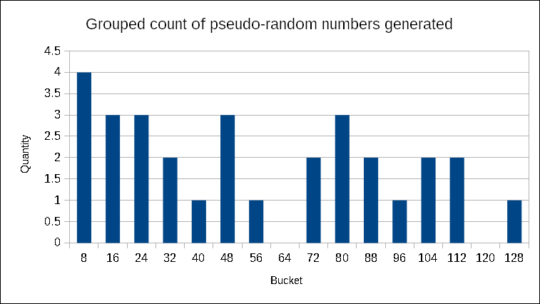
Unfortunately, 30 samples doesn’t allow for significant trends to develop in terms of frequency of occurance of various numbers. What this sample does show is that the LFSR is providing values throughout its full output range and, when I slowed down the clock to 1Hz, confirmed that it is operating exactly as it should.
Extra Features
Though functionally useless, I also added a scrolling message on the seven-segment display when the device turns on. In honor of CU, this message is go buffs.
I made this scroll across the available digits through the use of a 2Hz clock which causes the message to shift left by 8 bits (7 segments + decimal point).
Demonstration
Here is a video of the timer in action.
Further Development
This has been a really interesting experience getting to create low level hardware without ever having to physically manipulate hardware. I definitely have gained a bit more understanding as to the power of FPGAs despite the fact that I never came close to using even a single percent of this chip’s capability.
While I was working on this project I messed around a little bit with driving a VGA display since this hardware is fully capable of doing so. I never succeeded in producing a signal recognizable to my monitor, however I would like to investigate the cause of this failure in the future. It could be a good introduction to designing hardware for synchronous communication.
Resources
Due to this project being part of a course, I cannot publish the complete source code. If you are interested in seeing the source, please contact me directly.
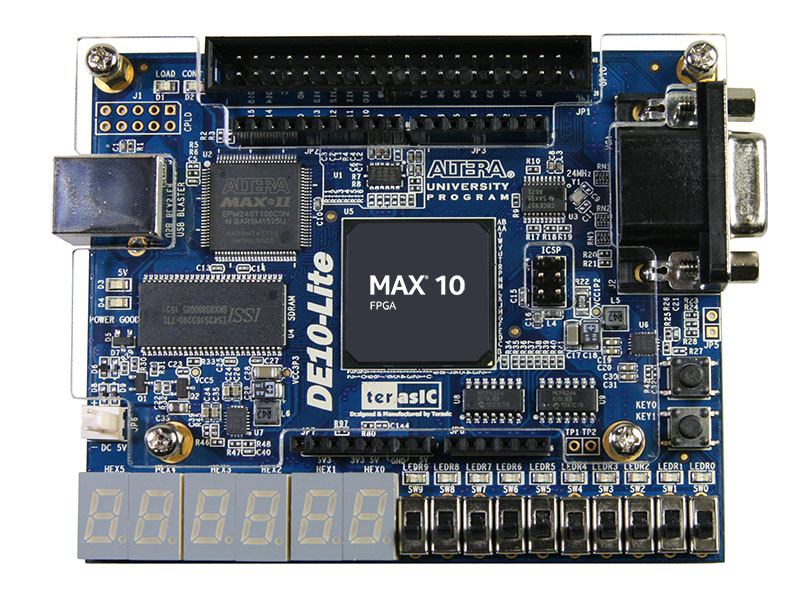
Information about the FPGA development board I used can be found on the manufacture’s website (http://de10-lite.terasic.com)